TiaC Magpie STM32F777NIHx
Overview
The TiaC Magpie STM32F777NIHx boards offer combinations of performance and power that provide an affordable and flexible way for users to build prototypes and try out new concepts target communication systems.
The board requires any separate JTAG/SWD probe, e.g. the ST-LINK/V2 debugger/programmer.
Key Features
STM32 microcontroller in TFBGA216 package
Ethernet compliant with IEEE-802.3-2002 (depending on STM32 support)
USB full-speed device (depending on STM32 support)
USB full-speed host with 7 port hub (depending on STM32 support)
2 user LEDs
reset push-button
25.000 MHz high-speed on-board crystal oscillator (for system clock)
32.768 kHz low-speed on-board crystal oscillator (for on-chip RTC)
Board connectors:
JTAG/SWD
UART Console over USB with Micro-AB
USB device with Micro-AB
Ethernet RJ45 (depending on STM32 support)
6 2x8 pin header with dedicated CAN and USB busses
5 2x7 TiaC Magpie compatible pin header with spare GPIO
Single power-supply input: 12V/3A external sources

Hardware
The STM32F777NIHx on the TiaC Magpie board provides the following hardware components:
STM32F777NIHx in TFBGA216 package
ARM 32-bit Cortex®-M7 CPU with DPFPU
Chrom-ART Accelerator
ART Accelerator
216 MHz max CPU frequency
VDD from 1.7 V to 3.6 V
2 MB Flash
512 KB SRAM
7-bit watchdog timer (1)
12-bit independent watchdog timer (1)
24-bit system-tick timer (1)
16-bit low-power timer (1)
16-bit timers (12)
32-bit timers (2)
SPI (6)
I2C (4)
I2S (3)
USART (4)
UART (4)
USB OTG Full Speed (1)
USB OTG Full Speed and High Speed (1)
10/100 Ethernet MAC with MII/RMII and MDIO (1)
CAN (3)
SAI (2)
Dual Mode Quad SPI (1)
GPIO (up to 168) with external interrupt capability
Digital Filters for Sigma Delta Modulator (DFSDM) with 8 channels / 4 filters
12-bit ADC with 24 channels / 2.4 MSPS (3)
12-bit DAC with 2 channels (2)
16-channel DMA
Cryptographic Acceleration for AES 128, 192, 256, triple DES, HASH (MD5, SHA-1, SHA-2), and HMAC
True Random Number Generator (RNG)
CRC calculation unit
RTC: subsecond accuracy, hardware calendar
96-bit unique ID
More information about the STM32F777NIHx can be found at the website about STM32F777NI on www.st.com [1] or in the STM32F777 Reference Manual (RM0410) [3] and the STM32F7 Series Cortex®-M7 Processor Programming Manual (PM0253) [2].
Supported Features
The Zephyr tiac_magpie board configuration supports the following
hardware features:
Interface |
Controller |
Driver/Component |
|---|---|---|
UART |
on-chip |
UART (!) (?) |
PINMUX |
on-chip |
|
GPIO |
on-chip |
|
ETH |
on-chip |
Ethernet (*) |
USB |
on-chip |
|
CAN |
on-chip |
|
I2C |
on-chip |
|
SPI |
on-chip |
SPI (?) |
PWM |
on-chip |
|
ADC |
on-chip |
ADC (+) (!) (?) |
RTC |
on-chip |
|
IWDG |
on-chip |
Watchdog (°) |
RNG |
on-chip |
|
RCC |
on-chip |
Reset & Clock Control |
NVIC |
on-chip |
Nested Vector Interrupts Controller |
- (*) Ethernet instability on SOC cut-A (Device marking A):
TiaC Magpie with SOC cut-A (Device marking A) has some ethernet instability (https://github.com/zephyrproject-rtos/zephyr/issues/26519). Use of cut-Z is advised. See restrictions errata: https://www.st.com/resource/en/errata_sheet/DM00257543.pdf
- (+) ADC 1 only supported:
ADC 2 or 3 is not supported properly by Zephyr STM32 ADC support, see: https://github.com/zephyrproject-rtos/zephyr/issues/26874 and https://github.com/zephyrproject-rtos/zephyr/issues/30977
- (-) CAN 1 or 2 only separate supported, never both simultaneously:
Simultaneous use of CAN_1 and CAN_2 not supported yet on STM32, see: https://github.com/zephyrproject-rtos/zephyr/blob/main/drivers/can/can_stm32.c#L26, https://github.com/zephyrproject-rtos/zephyr/pull/22200, https://github.com/zephyrproject-rtos/zephyr/pull/24396 and
- (!) Shared IRQ line on STM32 devices:
Share the same interrupt line on STM32 devices over multiple driver instances of same device class is not supported properly by Zephyr, see: https://github.com/zephyrproject-rtos/zephyr/issues/26874 and https://github.com/zephyrproject-rtos/zephyr/pull/27886
- (?) DMA transfer for STM32 devices:
Data cache invalidate/clean operation in DMA context is not properly integrated for STM32 devices, see: https://github.com/zephyrproject-rtos/zephyr/pull/27911, https://github.com/zephyrproject-rtos/zephyr/issues/29798, https://github.com/zephyrproject-rtos/zephyr/pull/32832 and https://github.com/zephyrproject-rtos/zephyr/issues/33485
- (°) IWDG only tested:
WWDG (Window Watchdog Timer) not yet part of board support, testet only with IWDG (Independent Watchdog Timer).
Other hardware features are not yet supported on this Zephyr board support.
The default configuration can be found in the defconfig file:
boards/arm/tiac_magpie/tiac_magpie_defconfig
Default Zephyr Peripheral Mapping:
The TiaC Magpie STM32F777NIHx board is configured as follows:
User LED 1/2 : PG11/PG12
JTAG(SWD) TMS/TCK/TDI/TDO/TRST : PA13/PA14/PA15/PB3/PB4 (ST-Link)
UART 7 TX/RX/RTS/CTS : PE8/PE7/PE9/PE10 (Zephyr Shell Console)
ETH : PA0, PA1, PA2, PA3, PA7, PB0, PB1, PB8, PB11, PC1, PC2, PC3, PC4, PC5, (PC6/PC7), PG13, PG14, PI10
USB OTG FS DM/DP (device) : PA11/PA12
USB OTG HS DM/DP (host/hub) : (PB14/PB15)
CAN 1 TX/RX : PH13/PH14, (PH15)
CAN 2 RX/TX : PB12/PB13, (PC9)
I2C 2 SDA/SCL : PF0/PF1
UART 4 TX/RX : PD1/PD0 (Shields)
I2C 4 SCL/SDA : PF14/PF15 (Shields)
SPI 5 MOSI/NSS/SCK/MISO : PF11/PH5/PH6/PH7 (Shields)
PWM TIM 8 CH1/2/3 : PI5/PI6/PI7 (Shields)
ADC 3 IN9/IN14/IN15 : PF3/PF4/PF5 (Shields)
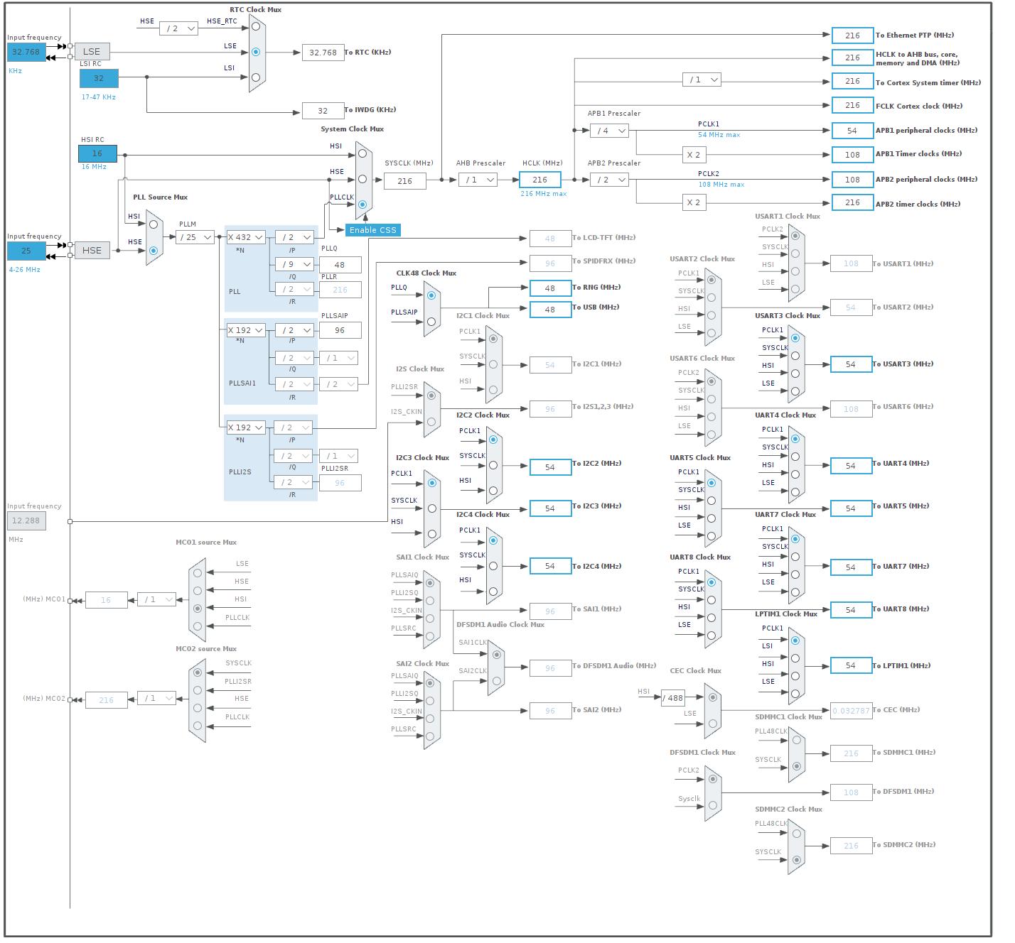
System and Real-Time Clock
The STM32F777NIHx System Clock on the TiaC Magpie board could be driven by an internal or external oscillator, as well as the main PLL clock. By default, the System clock is driven by the PLL clock at 216 MHz, driven by an 25 MHz high-speed on-board clock.
The STM32F777NIHx Real-Time Clock on the TiaC Magpie board could be driven by an internal or external oscillator. By default, the Real-Time Clock is driven by an 32.768 kHz low-speed on-board clock.
See System Clock with DTS Bindings and Kconfig for a more detailed specification.
User LED
The TiaC Magpie provides two red LEDs for user purposes.
See User LED with DTS Bindings for a more detailed specification.
Serial Port
The STM32F777NIHx on the TiaC Magpie board has 4 UARTs and 4 USARTs, but not all are open usable or accessible. The Zephyr console output is assigned to UART 7. Default settings are 115200 8N1 with hardware flow control (RTS/CTS).
See Serial Console with DTS Bindings for a more detailed specification.
Ethernet MAC
The STM32F777NIHx on the TiaC Magpie board has one 10/100 Ethernet MAC with MII/RMII and MDIO. The Zephyr network stack, mostly with TCP/IP support, is assigned to this MAC and will use the full MII with MDIO to communicate with the underlyed Ethernet PHY.
See Ethernet MAC with DTS Bindings for a more detailed specification.
USB OTG
The STM32F777NIHx on the TiaC Magpie board has two independent USB 2.0 OTG controller, one full-speed (FS) with an on-chip PHY and one high-speed (HS) or full-speed (FS) with an on-chip PHY and ULPI. Both controllers supports device or host mode. The TiaC Magpie uses the first USB 2.0 OTG FS controller in USB device mode. The second USB 2.0 OTG HS controller is reserved for USB host mode.
See USB OTG with DTS Bindings for a more detailed specification.
CAN Busses
The STM32F777NIHx on the TiaC Magpie board has 3 CAN controller, but not all are open usable or accessible. The TiaC Magpie uses the first two controllers, wherein the firstly enumerated is considered to be primarily.
Warning
With current Zephyr version, either CAN controller 1 or 2 can be used on their own, not both simultaneously.
The bus timing is defined by the DTS and is preset to 1000 kBit/s. The calculation was verified with the help of the CAN Bit Time Calculation Sheet [5] and can also assume smaller bit rates according to the following table. Note that the value of Prescaler will be calculated on demand by the driver.
Bit Rate |
Sample Point at |
Prescaler |
Seg 1 ( |
Seg 2 ( |
|---|---|---|---|---|
1000 kBit/s |
88.9 % |
3 |
15 |
2 |
500 kBit/s |
88.9 % |
6 |
15 |
2 |
250 kBit/s |
88.9 % |
12 |
15 |
2 |
125 kBit/s |
88.9 % |
24 |
15 |
2 |
125 kBit/s |
87.5 % |
27 |
13 |
2 |
100 kBit/s |
88.9 % |
30 |
15 |
2 |
50 kBit/s |
88.9 % |
60 |
15 |
2 |
20 kBit/s |
88.9 % |
150 |
15 |
2 |
10 kBit/s |
88.9 % |
300 |
15 |
2 |
See CAN Busses with DTS Bindings for a more detailed specification.
System I2C Bus
The STM32F777NIHx on the TiaC Magpie board has 4 I2C controller, but not
all are open usable or accessible. The TiaC Magpie uses the second controller
on-board for Power and Reset Controll on the 6 2x8 pin header, TUB[1..6].
See System I2C Bus with DTS Bindings for a more detailed specification.
Pin Header
The five TiaC Magpie pin headers TMPH[1..5] have the following layout:

See Pin Header with DTS Bindings for a more detailed specification.
Programming and Debugging
Applications for the tiac_magpie board configuration can be built and
flashed in the usual way (see Building an Application and
Run an Application for more details).
Flashing
The TiaC Magpie STM32F777NIHx needs an ST-LINK/V2 debug tool adapter.
Flashing an application to TiaC Magpie STM32F777NIHx
Here is an example for the Hello World application.
Run a serial host program to connect with your TiaC Magpie board.
$ screen /dev/ttyUSBx 115200,cs8,parenb,-parodd,-cstopb
Build and flash the application:
west build -b tiac_magpie -d build/hello_world-tiac_magpie zephyr/samples/hello_world
west flash -d build/hello_world-tiac_magpie
You should see the following message on the console:
*** Booting Zephyr OS version x.y.z  ***
Hello World! tiac_magpie
Debugging
You can debug an application in the usual way. Here is an example for the Hello World application.
# From the root of the zephyr repository
west build -b tiac_magpie -d build/hello_world-tiac_magpie zephyr/samples/hello_world
west debug -d build/hello_world-tiac_magpie
Tests and Examples
Examples and Demonstrations
Zephyr provides a large number of samples and demonstration applications, some of which can be used for the start-up of the TiaC Magpie without any further modification:
Integration Tests
Zephyr provides a large number of integration tests to evaluate the target architecture, the operating system core components, drivers and subsystems. Most of them can be build and running by the Zephyr Test Runner (Twister) without any further modification.
Before a single or multiple test cases can be executed directly on the TiaC Magpie, a so-called hardware map must be created with the help of Twister and adapted manually. You can do that with the following command line inside your local workspace directory:
$ rm -f map.yaml && cd ./zephyr && \
    ./scripts/twister --generate-hardware-map ../map.yaml && \
    cd - && editor map.yaml
This hardware map (map.yaml) could look like the following. Bold
highlighted portions need to be added manually. Italic parts have to be
adapted to your own specific situation, important here is the platform
setup to tiac_magpie.
- available: true
  connected: true
  fixtures:
    - gpio_loopback
    - pwm_loopback
    - spi_loopback
    - i2c_bus_short
  id: DT04BNT1
  platform: tiac_magpie
  product: FT230X Basic UART
  runner: openocd
  serial: /dev/ttyUSB0
All currently qualified tests for TiaC Magpie can be executed and verified with a single call to Twister.
Attention
This will take more than a quarter of an hour.
Build and run the tests on target as follows:
$ ./zephyr/scripts/twister --jobs 4 \
    --enable-size-report --platform-reports \
    --device-testing --hardware-map map.yaml \
    --extra-args SHIELD="loopback_test_tmph can_timing_adj" \
    --board-root bridle/boards \
    --testsuite-root bridle/tests/bridle \
    --testsuite-root zephyr/tests/kernel \
    --testsuite-root zephyr/tests/arch/arm \
    --testsuite-root zephyr/tests/crypto/rand32 \
    --testsuite-root zephyr/tests/drivers/entropy \
    --testsuite-root zephyr/tests/drivers/watchdog \
    --testsuite-root bridle/tests/drivers/watchdog \
    --testsuite-root zephyr/tests/drivers/counter \
    --testsuite-root zephyr/tests/drivers/hwinfo \
    --testsuite-root zephyr/tests/drivers/uart \
    --testsuite-root zephyr/tests/drivers/gpio \
    --testsuite-root zephyr/tests/drivers/spi \
    --testsuite-root zephyr/tests/drivers/can
You should see the following messages on host console:
Device testing on:

| Platform    | ID       | Serial device   |
|-------------|----------|-----------------|
| tiac_magpie | DT04BNT1 | /dev/ttyUSB0    |

INFO    - Adding tasks to the queue...
INFO    - Added initial list of jobs to queue

INFO    - Total complete:  266/ 266  100%  skipped:   143, failed:    0

INFO    - 266 test scenarios (266 test instances) selected, 143 configurations skipped (118 by static filter, 25 at runtime).
INFO    - 123 of 266 test configurations passed (100.00%), 0 failed, 143 skipped with 0 warnings in 1760.04 seconds
INFO    - In total 1194 test cases were executed, 747 skipped on 1 out of total 541 platforms (0.18%)
INFO    - 123 test configurations executed on platforms, 0 test configurations were only built.

Hardware distribution summary:

| Board       | ID       |   Counter |
|-------------|----------|-----------|
| tiac_magpie | DT04BNT1 |       123 |
Known but currently tolerated test cases with errors
Likewise, each of these test suites can also be running individually. The following are valid:
Detailed Specification
System Clock with DTS Bindings and Kconfig
The DTS binding following the st,stm32-rcc,
st,stm32f7-pll-clock, st,stm32-hse-clock
and st,stm32-lse-clock specification. The Kconfig default
configuration is for STM32 RTC (Real-Time Clock Controller) and will be used
by counter driver behind DTS binding following the st,stm32-rtc
specification.
Clock-Tree |
DTS Bindings / Kconfig |
|---|---|
|
tiac_magpie.dts
1&clk_hse {
2	status = "okay";
3	clock-frequency = <DT_FREQ_M(25)>;
4	hse-bypass;
5}; // clk_hse
tiac_magpie.dts
1&pll {
2	status = "okay";
3	clocks = <&clk_hse>;
4	div-m = <25>;
5	mul-n = <432>;
6	div-p = <2>;
7	div-q = <9>;
8}; // pll
tiac_magpie.dts
1&rcc {
2	status = "okay";
3	clocks = <&pll>;
4	ahb-prescaler = <1>;
5	apb1-prescaler = <4>;
6	apb2-prescaler = <2>;
7	clock-frequency = <DT_FREQ_M(216)>;
8}; // rcc
tiac_magpie.dts
1&clk_lse {
2	status = "okay";
3	clock-frequency = <DT_FREQ_K(32)>;
4	lse-bypass;
5}; // clk_lse
tiac_magpie.dts
1&rtc {
2	status = "okay";
3	clocks = <&rcc STM32_CLOCK_BUS_APB1 0x10000000>,
4		 <&rcc STM32_SRC_LSE RTC_SEL(1)>;
5}; // rtc
tiac_magpie_defconfig
1# Clock Configuration
2CONFIG_CLOCK_CONTROL=y
3
4# RTC Counter
5CONFIG_COUNTER=y
|
User LED with DTS Bindings
The DTS binding following the gpio-leds specification.
Multiplexing |
Device-Tree |
|||||||||
|---|---|---|---|---|---|---|---|---|---|---|
|
tiac_magpie.dts
 1	leds {
 2		compatible = "gpio-leds";
 3		usr_led_1: usr_led_1 {
 4			gpios = <&gpiog 11 GPIO_ACTIVE_HIGH>;	/* USER_LED1 */
 5			label = "User LED1";
 6		}; // usr_led_1
 7		usr_led_2: usr_led_2 {
 8			gpios = <&gpiog 12 GPIO_ACTIVE_HIGH>;	/* USER_LED2 */
 9			label = "User LED2";
10		}; // usr_led_2
11	}; // leds
DTS aliases: led0 = &usr_led_1;
led1 = &usr_led_2;
|
Serial Console with DTS Bindings
The DTS binding following the st,stm32-uart specification.
Multiplexing |
Device-Tree |
|||||||||||||||
|---|---|---|---|---|---|---|---|---|---|---|---|---|---|---|---|---|
|
tiac_magpie.dts
 1&uart7 {
 2	status = "okay";		/* default system uart console */
 3	pinctrl-names = "default";
 4	pinctrl-0 = <&uart7_tx_pe8	/* UART_TXD7 */
 5		     &uart7_rx_pe7	/* UART_RXD7 */
 6		     &uart7_rts_pe9	/* UART_RTS7 */
 7		     &uart7_cts_pe10>;	/* UART_CTS7 */
 8	current-speed = <115200>;
 9	hw-flow-control;
10}; // uart7
zephyr,console = &uart7;
zephyr,shell-uart = &uart7;
|
Ethernet MAC with DTS Bindings
The DTS binding following the st,stm32-ethernet specification.
Multiplexing |
Device-Tree |
||||||||||||||||||||||||||||||||||||||||||||||||||||||||||||
|---|---|---|---|---|---|---|---|---|---|---|---|---|---|---|---|---|---|---|---|---|---|---|---|---|---|---|---|---|---|---|---|---|---|---|---|---|---|---|---|---|---|---|---|---|---|---|---|---|---|---|---|---|---|---|---|---|---|---|---|---|---|
|
tiac_magpie.dts
1&mac {
2 status = "okay";
3 pinctrl-names = "default";
4 pinctrl-0 = <ð_mdc_pc1 /* MII_MDC */
5 ð_mdio_pa2 /* MII_MDIO */
6 ð_col_pa3 /* MII_COL */
7 ð_crs_pa0 /* MII_CRS */
8 ð_txd3_pb8 /* MII_TXD3 */
9 ð_txd2_pc2 /* MII_TXD2 */
10 ð_txd1_pg14 /* MII_TXD1 */
11 ð_txd0_pg13 /* MII_TXD0 */
12 ð_tx_en_pb11 /* MII_TXEN */
13 ð_tx_clk_pc3 /* MII_TXC */
14 ð_rx_er_pi10 /* MII_RXER */
15 ð_rxd3_pb1 /* MII_RXD3 */
16 ð_rxd2_pb0 /* MII_RXD2 */
17 ð_rxd1_pc5 /* MII_RXD1 */
18 ð_rxd0_pc4 /* MII_RXD0 */
19 ð_rx_dv_pa7 /* MII_RXDV */
20 ð_rx_clk_pa1>; /* MII_RXC */
21}; // mac
|
USB OTG with DTS Bindings
The DTS binding following the st,stm32-otgfs and
st,stm32-otghs specification.
Multiplexing |
Device-Tree |
|||||||||
|---|---|---|---|---|---|---|---|---|---|---|
|
tiac_magpie.dts
1&usbotg_fs {
2	status = "okay";
3	pinctrl-names = "default";
4	pinctrl-0 = <&usb_otg_fs_dm_pa11	/* USB_DEV_DP */
5		     &usb_otg_fs_dp_pa12>;	/* USB_DEV_DM */
6}; // usbotg_fs
USB device support configuration: zephyr,usb-device = &usbotg_fs;
|
|||||||||
|
Not yet configured! Only USB device function is supported in Zephyr at the moment
Since end of 2020 there is an PR with experimental USB host
support for Zephyr – but that must be checked in detail
|
CAN Busses with DTS Bindings
The DTS binding following the st,stm32-can specification.
Multiplexing |
Device-Tree |
||||||||||||
|---|---|---|---|---|---|---|---|---|---|---|---|---|---|
|
tiac_magpie.dts
 1&can1 {
 2	status = "okay";		/* default primary can */
 3	pinctrl-names = "default";
 4	pinctrl-0 = <&can1_rx_ph14	/* CAN_RX1 */
 5		     &can1_tx_ph13>;	/* CAN_TX1 */
 6	bus-speed = <1000000>;
 7	sjw = <1>;
 8	prop-seg = <0>;
 9	phase-seg1 = <15>;
10	phase-seg2 = <2>;
11}; // can1
CAN Controller configuration: zephyr,canbus = &can1;
|
||||||||||||
|
tiac_magpie.dts
 1&can2 {
 2	status = "disabled";		/* optional second can */
 3	pinctrl-names = "default";
 4	pinctrl-0 = <&can2_rx_pb12	/* CAN_RX2 */
 5		     &can2_tx_pb13>;	/* CAN_TX2 */
 6	bus-speed = <1000000>;
 7	sjw = <1>;
 8	prop-seg = <0>;
 9	phase-seg1 = <15>;
10	phase-seg2 = <2>;
11}; // can2
|
System I2C Bus with DTS Bindings
The DTS binding following the st,stm32-i2c-v2 specification.
Multiplexing |
Device-Tree |
|||||||||
|---|---|---|---|---|---|---|---|---|---|---|
|
tiac_magpie.dts
1&i2c2 {
2	status = "okay";		/* default system i2c */
3	pinctrl-names = "default";
4	pinctrl-0 = <&i2c2_scl_pf1	/* SCL2 */
5		     &i2c2_sda_pf0>;	/* SDA2 */
6	clock-frequency = <I2C_BITRATE_FAST>;
7}; // i2c2
|
Pin Header with DTS Bindings
The TiaC Magpie compatible pin header expands functionality of the TiaC
development platform, with a wide choice of specialized TiaC shields.
The DTS binding following the tiac-magpie-pin-header
specification.
TiaC Magpie Pin Header 1
Alternate functions on the TiaC Magpie pin header TMPH1:
Label |
Name |
Signal |
AF1 |
AF2 |
AF3 |
AF5 |
AF6 |
AF7 |
AF8 |
|---|---|---|---|---|---|---|---|---|---|
TMPH1_PC12_TXD5 |
PC12 |
UART5_TX |
I2S3_SD/SPI3_MOSI |
USART3_CK |
UART5_TX |
||||
TMPH1_PD0_RXD4 |
PD0 |
UART4_RX |
DFSDM1_CKIN6 |
DFSDM1_DATIN7 |
UART4_RX |
||||
TMPH1_PC11_RXD3 |
PC11 |
USART3_RX |
DFSDM1_DATIN5 |
SPI3_MISO |
USART3_RX |
UART4_RX |
|||
TMPH1_PC10_TXD3 |
PC10 |
USART3_TX |
DFSDM1_CKIN5 |
I2S3_CK/SPI3_SCK |
USART3_TX |
UART4_TX |
|||
TMPH1_PD3 |
PD3 |
GPIO_Analog |
DFSDM1_CKOUT |
I2S2_CK/SPI2_SCK |
DFSDM1_DATIN0 |
USART2_CTS |
|||
TMPH1_PD1_TXD4 |
PD1 |
UART4_TX |
DFSDM1_DATIN6 |
DFSDM1_CKIN7 |
UART4_TX |
||||
TMPH1_PI3 |
PI3 |
GPIO_Analog |
TIM8_ETR |
I2S2_SD/SPI2_MOSI |
|||||
TMPH1_PI2_PWM84 |
PI2 |
TIM8_CH4 |
TIM8_CH4 |
SPI2_MISO |
|||||
TMPH1_PD4 |
PD4 |
GPIO_Analog |
DFSDM1_CKIN0 |
USART2_DE/USART2_RTS |
|||||
TMPH1_PD2_RXD5 |
PD2 |
UART5_RX |
TIM3_ETR |
UART5_RX |
|||||
TMPH1_PA10 |
PA10 |
GPIO_Analog |
TIM1_CH3 |
USART1_RX |
|||||
TMPH1_PI9 |
PI9 |
GPIO_Analog |
UART4_RX |
Relationship |
Device-Tree |
|---|---|
 |
tiac_magpie_pin_header.dtsi
 1	tmph1: tmph1-connector {
 2		compatible = "tiac-magpie-pin-header";
 3		#gpio-cells = <2>;
 4		gpio-map-mask = <0xffffffff 0xffffffc0>;
 5		gpio-map-pass-thru = <0 0x3f>;
 6		gpio-map = <0 0 &gpioa 10 0>,	/* TMPH1_PA10 */
 7			   <1 0 &gpioi 3 0>,	/* TMPH1_PI3 */
 8			   <2 0 &gpioi 2 0>,	/* TMPH1_PI2_PWM84 */
 9			   <3 0 &gpioc 10 0>,	/* TMPH1_PC10_TXD3 */
10			   <4 0 &gpioc 11 0>,	/* TMPH1_PC11_RXD3 */
11			   <5 0 &gpiod 2 0>,	/* TMPH1_PD2_RXD5 */
12			   <6 0 &gpiod 0 0>,	/* TMPH1_PD0_RXD4 */
13			   <7 0 &gpioc 12 0>,	/* TMPH1_PC12_TXD5 */
14			   <8 0 &gpiod 1 0>,	/* TMPH1_PD1_TXD4 */
15			   <9 0 &gpiod 3 0>,	/* TMPH1_PD3 */
16			   <10 0 &gpiod 4 0>,	/* TMPH1_PD4 */
17			   <11 0 &gpioi 9 0>;	/* TMPH1_PI9 */
18			   /* Not a GPIO*/	/* GND */
19			   /* Not a GPIO*/	/* GND */
20	}; // tmph1
|
tmph_serial: &tmph_serial1 {};
tmph_serial1: &uart4 {};
|
tiac_magpie.dts
1&uart4 {
2	status = "okay";		/* default primary uart */
3	pinctrl-names = "default";
4	pinctrl-0 = <&uart4_tx_pd1	/* TMPH1_PD1_TXD4 */
5		     &uart4_rx_pd0>;	/* TMPH1_PD0_RXD4 */
6	current-speed = <115200>;
7}; // uart4
|
tmph_serial2: &usart3 {};
|
tiac_magpie.dts
1&usart3 {
2	status = "disabled";		/* optional second uart */
3	pinctrl-names = "default";
4	pinctrl-0 = <&usart3_tx_pc10	/* TMPH1_PC10_TXD3 */
5		     &usart3_rx_pc11>;	/* TMPH1_PC11_RXD3 */
6	current-speed = <115200>;
7}; // usart3
|
tmph_serial3: &uart5 {};
|
tiac_magpie.dts
1&uart5 {
2	status = "disabled";		/* optional third uart */
3	pinctrl-names = "default";
4	pinctrl-0 = <&uart5_tx_pc12	/* TMPH1_PC12_TXD5 */
5		     &uart5_rx_pd2>;	/* TMPH1_PD2_RXD5 */
6	current-speed = <115200>;
7}; // uart5
|
tmph_timers: &timers8 {};
tmph_pwms: &pwm8 {};
|
tiac_magpie.dts
 1&timers8 {
 2	status = "okay";
 3
 4	pwm8: pwm {
 5		status = "okay";
 6		pinctrl-names = "default";
 7		pinctrl-0 = <&tim8_ch1_pi5	/* TMPH4_PI5_PWM81 */
 8			     &tim8_ch2_pi6	/* TMPH4_PI6_PWM82 */
 9			     &tim8_ch3_pi7 	/* TMPH4_PI7_PWM83 */
10			     &tim8_ch4_pi2>;	/* TMPH1_PI2_PWM84 */
11	}; // pwm8
12}; // timers8
|
TiaC Magpie Pin Header 2
Alternate functions on the TiaC Magpie pin header TMPH2:
Label |
Name |
Signal |
AF1 |
AF2 |
AF3 |
AF4 |
AF5 |
AF7 |
AF8 |
|---|---|---|---|---|---|---|---|---|---|
TMPH2_PI1 |
PI1 |
GPIO_Analog |
TIM8_BKIN2 |
I2S2_CK/SPI2_SCK |
|||||
TMPH2_PI0 |
PI0 |
GPIO_Analog |
TIM5_CH4 |
I2S2_WS/SPI2_NSS |
|||||
TMPH2_PA9 |
PA9 |
GPIO_Analog |
TIM1_CH2 |
I2C3_SMBA |
I2S2_CK/SPI2_SCK |
USART1_TX |
|||
TMPH2_PI15 |
PI15 |
GPIO_Analog |
|||||||
TMPH2_PG8 |
PG8 |
GPIO_Analog |
SPI6_NSS |
SPDIFRX_IN2 |
USART6_DE/USART6_RTS |
||||
TMPH2_PF4_ADC314 |
PF4 |
GPIO_Analog ADC3_IN14 |
|||||||
TMPH2_PH5_NSS5 |
PH5 |
SPI5_NSS |
I2C2_SDA |
SPI5_NSS |
|||||
TMPH2_PH3 |
PH3 |
GPIO_Analog |
|||||||
TMPH2_PF5_ADC315 |
PF5 |
GPIO_Analog ADC3_IN15 |
|||||||
TMPH2_PD15_RTS8 |
PD15 |
UART8_RTS |
TIM4_CH4 |
UART8_DE/UART8_RTS |
|||||
TMPH2_PD10 |
PD10 |
GPIO_Analog |
DFSDM1_CKOUT |
USART3_CK |
|||||
TMPH2_PD14_CTS8 |
PD14 |
UART8_CTS |
TIM4_CH3 |
UART8_CTS |
Relationship |
Device-Tree |
|---|---|
 |
tiac_magpie_pin_header.dtsi
 1	tmph2: tmph2-connector {
 2		compatible = "tiac-magpie-pin-header";
 3		#gpio-cells = <2>;
 4		gpio-map-mask = <0xffffffff 0xffffffc0>;
 5		gpio-map-pass-thru = <0 0x3f>;
 6		gpio-map = <0 0 &gpiod 10 0>,	/* TMPH2_PD10 */
 7			   <1 0 &gpiod 14 0>,	/* TMPH2_PD14_CTS8 */
 8			   <2 0 &gpiod 15 0>,	/* TMPH2_PD15_RTS8 */
 9			   <3 0 &gpiof 5 0>,	/* TMPH2_PF5_ADC315 */
10			   <4 0 &gpiog 8 0>,	/* TMPH2_PG8 */
11			   <5 0 &gpioh 3 0>,	/* TMPH2_PH3 */
12			   <6 0 &gpioh 5 0>,	/* TMPH2_PH5_NSS5 */
13			   <7 0 &gpiof 4 0>,	/* TMPH2_PF4_ADC314 */
14			   <8 0 &gpioi 15 0>,	/* TMPH2_PI15 */
15			   <9 0 &gpioi 0 0>,	/* TMPH2_PI0 */
16			   <10 0 &gpioa 9 0>,	/* TMPH2_PA9 */
17			   <11 0 &gpioi 1 0>;	/* TMPH2_PI1 */
18			   /* Not a GPIO*/	/* GND */
19			   /* Not a GPIO*/	/* GND */
20	}; // tmph2
|
tmph_serial4: &uart8 {};
|
tiac_magpie.dts
1&uart8 {
2	status = "disabled";		/* optional fourth uart */
3	pinctrl-names = "default";
4	pinctrl-0 = <&uart8_tx_pe1	/* TMPH4_PE1_TXD8 */
5		     &uart8_rx_pe0	/* TMPH4_PE0_RXD8 */
6		     &uart8_rts_pd15	/* TMPH2_PD15_RTS8 */
7		     &uart8_cts_pd14>;	/* TMPH2_PD14_CTS8 */
8	current-speed = <115200>;
9}; // uart8
|
tmph_spi2: &spi5 {};
|
tiac_magpie.dts
1&spi5 {
2	status = "disabled";		/* optional second spi */
3	pinctrl-names = "default";
4	pinctrl-0 = <&spi5_nss_ph5	/* TMPH2_PH5_NSS5 */
5		     &spi5_sck_ph6	/* TMPH3_PH6_SCK5 */
6		     &spi5_miso_ph7	/* TMPH3_PH7_SCL3_MISO5 */
7		     &spi5_mosi_pf11>;	/* TMPH5_PF11_MOSI5 */
8}; // spi5
|
tmph_adc: &adc3 {};
|
tiac_magpie.dts
1&adc3 {
2	status = "okay";
3	pinctrl-names = "default";
4	pinctrl-0 = <&adc3_in9_pf3	/* TMPH4_PF3_ADC39 */
5		     &adc3_in14_pf4	/* TMPH2_PF4_ADC314 */
6		     &adc3_in15_pf5>;	/* TMPH2_PF5_ADC315 */
7}; // adc3
|
TiaC Magpie Pin Header 3
Alternate functions on the TiaC Magpie pin header TMPH3:
Label |
Name |
Signal |
AF2 |
AF3 |
AF4 |
AF5 |
AF9 |
|---|---|---|---|---|---|---|---|
TMPH3_PH2 |
PH2 |
GPIO_Analog |
LPTIM1_IN2 |
QUADSPI_BK2_IO0 |
|||
TMPH3_PG3 |
PG3 |
GPIO_Analog |
|||||
TMPH3_PG2 |
PG2 |
GPIO_Analog |
|||||
TMPH3_PH12 |
PH12 |
GPIO_Analog |
TIM5_CH3 |
I2C4_SDA |
|||
TMPH3_PG5 |
PG5 |
GPIO_Analog |
|||||
TMPH3_PG4 |
PG4 |
GPIO_Analog |
|||||
TMPH3_PH7_SCL3_MISO5 |
PH7 |
I2C3_SCL |
I2C3_SCL |
SPI5_MISO |
|||
TMPH3_PH9 |
PH9 |
GPIO_Analog |
I2C3_SMBA |
TIM12_CH2 |
|||
TMPH3_PH11 |
PH11 |
GPIO_Analog |
TIM5_CH2 |
I2C4_SCL |
|||
TMPH3_PH6_SCK5 |
PH6 |
SPI5_SCK |
I2C2_SMBA |
SPI5_SCK |
TIM12_CH1 |
||
TMPH3_PH8_SDA3 |
PH8 |
I2C3_SDA |
I2C3_SDA |
||||
TMPH3_PH10 |
PH10 |
GPIO_Analog |
TIM5_CH1 |
I2C4_SMBA |
Relationship |
Device-Tree |
|---|---|
 |
tiac_magpie_pin_header.dtsi
 1	tmph3: tmph3-connector {
 2		compatible = "tiac-magpie-pin-header";
 3		#gpio-cells = <2>;
 4		gpio-map-mask = <0xffffffff 0xffffffc0>;
 5		gpio-map-pass-thru = <0 0x3f>;
 6		gpio-map = <0 0 &gpiog 5 0>,	/* TMPH3_PG5 */
 7			   <1 0 &gpiog 4 0>,	/* TMPH3_PG4 */
 8			   <2 0 &gpioh 6 0>,	/* TMPH3_PH6_SCK5 */
 9			   <3 0 &gpioh 8 0>,	/* TMPH3_PH8_SDA3 */
10			   <4 0 &gpioh 10 0>,	/* TMPH3_PH10 */
11			   <5 0 &gpioh 9 0>,	/* TMPH3_PH9 */
12			   <6 0 &gpioh 11 0>,	/* TMPH3_PH11 */
13			   <7 0 &gpioh 7 0>,	/* TMPH3_PH7_SCL3_MISO5 */
14			   <8 0 &gpioh 12 0>,	/* TMPH3_PH12 */
15			   <9 0 &gpiog 2 0>,	/* TMPH3_PG2 */
16			   <10 0 &gpiog 3 0>,	/* TMPH3_PG3 */
17			   <11 0 &gpioh 2 0>;	/* TMPH3_PH2 */
18			   /* Not a GPIO*/	/* GND */
19			   /* Not a GPIO*/	/* GND */
20	}; // tmph3
|
tmph_i2c2: &i2c3 {};
|
tiac_magpie.dts
1&i2c3 {
2	status = "disabled";		/* optional second i2c */
3	pinctrl-names = "default";
4	pinctrl-0 = <&i2c3_scl_ph7	/* TMPH3_PH7_SCL3_MISO5 */
5		     &i2c3_sda_ph8>;	/* TMPH3_PH8_SDA3 */
6	clock-frequency = <I2C_BITRATE_STANDARD>;
7}; // i2c3
|
tmph_spi2: &spi5 {};
|
tiac_magpie.dts
1&spi5 {
2	status = "disabled";		/* optional second spi */
3	pinctrl-names = "default";
4	pinctrl-0 = <&spi5_nss_ph5	/* TMPH2_PH5_NSS5 */
5		     &spi5_sck_ph6	/* TMPH3_PH6_SCK5 */
6		     &spi5_miso_ph7	/* TMPH3_PH7_SCL3_MISO5 */
7		     &spi5_mosi_pf11>;	/* TMPH5_PF11_MOSI5 */
8}; // spi5
|
TiaC Magpie Pin Header 4
Alternate functions on the TiaC Magpie pin header TMPH4:
Label |
Name |
Signal |
AF2 |
AF3 |
AF4 |
AF8 |
|---|---|---|---|---|---|---|
TMPH4_PE1_TXD8 |
PE1 |
UART8_TX |
LPTIM1_IN2 |
UART8_TX |
||
TMPH4_PE0_RXD8 |
PE0 |
UART8_RX |
TIM4_ETR |
LPTIM1_ETR |
UART8_RX |
|
TMPH4_PG15 |
PG15 |
GPIO_Analog |
USART6_CTS |
|||
TMPH4_PI4 |
PI4 |
GPIO_Analog |
TIM8_BKIN |
|||
TMPH4_PI5_PWM81 |
PI5 |
TIM8_CH1 |
TIM8_CH1 |
|||
TMPH4_PI7_PWM83 |
PI7 |
TIM8_CH3 |
TIM8_CH3 |
|||
TMPH4_PI6_PWM82 |
PI6 |
TIM8_CH2 |
TIM8_CH2 |
|||
TMPH4_PI12 |
PI12 |
GPIO_Analog |
||||
TMPH4_PF2 |
PF2 |
GPIO_Analog |
I2C2_SMBA |
|||
TMPH4_PI13 |
PI13 |
GPIO_Analog |
||||
TMPH4_PF3_ADC39 |
PF3 |
GPIO_Analog ADC3_IN9 |
||||
TMPH4_PI14 |
PI14 |
GPIO_Analog |
Relationship |
Device-Tree |
|---|---|
 |
tiac_magpie_pin_header.dtsi
 1	tmph4: tmph4-connector {
 2		compatible = "tiac-magpie-pin-header";
 3		#gpio-cells = <2>;
 4		gpio-map-mask = <0xffffffff 0xffffffc0>;
 5		gpio-map-pass-thru = <0 0x3f>;
 6		gpio-map = <0 0 &gpioi 6 0>,	/* TMPH4_PI6_PWM82 */
 7			   <1 0 &gpioi 14 0>,	/* TMPH4_PI14 */
 8			   <2 0 &gpioi 7 0>,	/* TMPH4_PI7_PWM83 */
 9			   <3 0 &gpioi 12 0>,	/* TMPH4_PI12 */
10			   <4 0 &gpioi 5 0>,	/* TMPH4_PI5_PWM81 */
11			   <5 0 &gpiog 15 0>,	/* TMPH4_PG15 */
12			   <6 0 &gpioi 13 0>,	/* TMPH4_PI13 */
13			   <7 0 &gpiof 2 0>,	/* TMPH4_PF2 */
14			   <8 0 &gpioe 0 0>,	/* TMPH4_PE0_RXD8 */
15			   <9 0 &gpiof 3 0>,	/* TMPH4_PF3_ADC39 */
16			   <10 0 &gpioe 1 0>,	/* TMPH4_PE1_TXD8 */
17			   <11 0 &gpioi 4 0>;	/* TMPH4_PI4 */
18			   /* Not a GPIO*/	/* GND */
19			   /* Not a GPIO*/	/* GND */
20	}; // tmph4
|
tmph_serial4: &uart8 {};
|
tiac_magpie.dts
1&uart8 {
2	status = "disabled";		/* optional fourth uart */
3	pinctrl-names = "default";
4	pinctrl-0 = <&uart8_tx_pe1	/* TMPH4_PE1_TXD8 */
5		     &uart8_rx_pe0	/* TMPH4_PE0_RXD8 */
6		     &uart8_rts_pd15	/* TMPH2_PD15_RTS8 */
7		     &uart8_cts_pd14>;	/* TMPH2_PD14_CTS8 */
8	current-speed = <115200>;
9}; // uart8
|
tmph_timers: &timers8 {};
tmph_pwms: &pwm8 {};
|
tiac_magpie.dts
 1&timers8 {
 2	status = "okay";
 3
 4	pwm8: pwm {
 5		status = "okay";
 6		pinctrl-names = "default";
 7		pinctrl-0 = <&tim8_ch1_pi5	/* TMPH4_PI5_PWM81 */
 8			     &tim8_ch2_pi6	/* TMPH4_PI6_PWM82 */
 9			     &tim8_ch3_pi7 	/* TMPH4_PI7_PWM83 */
10			     &tim8_ch4_pi2>;	/* TMPH1_PI2_PWM84 */
11	}; // pwm8
12}; // timers8
|
tmph_adc: &adc3 {};
|
tiac_magpie.dts
1&adc3 {
2	status = "okay";
3	pinctrl-names = "default";
4	pinctrl-0 = <&adc3_in9_pf3	/* TMPH4_PF3_ADC39 */
5		     &adc3_in14_pf4	/* TMPH2_PF4_ADC314 */
6		     &adc3_in15_pf5>;	/* TMPH2_PF5_ADC315 */
7}; // adc3
|
TiaC Magpie Pin Header 5
Alternate functions on the TiaC Magpie pin header TMPH5:
Label |
Name |
Signal |
AF1 |
AF4 |
AF5 |
|---|---|---|---|---|---|
TMPH5_PF12 |
PF12 |
GPIO_Analog |
|||
TMPH5_PG1 |
PG1 |
GPIO_Analog |
|||
TMPH5_PF15_SDA4 |
PF15 |
I2C4_SDA |
I2C4_SDA |
||
TMPH5_PF13_SMBA4 |
PF13 |
I2C4_SMBA |
I2C4_SMBA |
||
TMPH5_PG0 |
PG0 |
GPIO_Analog |
|||
TMPH5_PF14_SCL4 |
PF14 |
I2C4_SCL |
I2C4_SCL |
||
TMPH5_PF11_MOSI5 |
PF11 |
SPI5_MOSI |
SPI5_MOSI |
||
TMPH5_PE11_NSS4 |
PE11 |
SPI4_NSS |
TIM1_CH2 |
SPI4_NSS |
|
TMPH5_PE14_MOSI4 |
PE14 |
SPI4_MOSI |
TIM1_CH4 |
SPI4_MOSI |
|
TMPH5_PE12_SCK4 |
PE12 |
SPI4_SCK |
TIM1_CH3N |
SPI4_SCK |
|
TMPH5_PE15 |
PE15 |
GPIO_Analog |
TIM1_BKIN |
||
TMPH5_PE13_MISO4 |
PE13 |
SPI4_MISO |
TIM1_CH3 |
SPI4_MISO |
Relationship |
Device-Tree |
|---|---|
 |
tiac_magpie_pin_header.dtsi
 1	tmph5: tmph5-connector {
 2		compatible = "tiac-magpie-pin-header";
 3		#gpio-cells = <2>;
 4		gpio-map-mask = <0xffffffff 0xffffffc0>;
 5		gpio-map-pass-thru = <0 0x3f>;
 6		gpio-map = <0 0 &gpiof 14 0>,	/* TMPH5_PF14_SCL4 */
 7			   <1 0 &gpiof 13 0>,	/* TMPH5_PF13 */
 8			   <2 0 &gpiof 12 0>,	/* TMPH5_PF12 */
 9			   <3 0 &gpiog 0 0>,	/* TMPH5_PG0 */
10			   <4 0 &gpiog 1 0>,	/* TMPH5_PG1 */
11			   <5 0 &gpiof 11 0>,	/* TMPH5_PF11_MOSI5 */
12			   <6 0 &gpiof 15 0>,	/* TMPH5_PF15_SDA4 */
13			   <7 0 &gpioe 12 0>,	/* TMPH5_PE12_SCK4 */
14			   <8 0 &gpioe 11 0>,	/* TMPH5_PE11_NSS4 */
15			   <9 0 &gpioe 15 0>,	/* TMPH5_PE15 */
16			   <10 0 &gpioe 14 0>,	/* TMPH5_PE14_MOSI4 */
17			   <11 0 &gpioe 13 0>;	/* TMPH5_PE13_MISO4 */
18			   /* Not a GPIO*/	/* GND */
19			   /* Not a GPIO*/	/* GND */
20	}; // tmph5
|
tmph_i2c: &tmph_i2c1 {};
tmph_i2c1: &i2c4 {};
|
tiac_magpie.dts
1&i2c4 {
2	status = "okay";		/* default primary i2c */
3	pinctrl-names = "default";
4	pinctrl-0 = <&i2c4_scl_pf14	/* TMPH5_PF14_SCL4 */
5		     &i2c4_sda_pf15>;	/* TMPH5_PF15_SDA4 */
6	clock-frequency = <I2C_BITRATE_STANDARD>;
7}; // i2c4
|
tmph_spi: &tmph_spi1 {};
tmph_spi1: &spi4 {};
|
tiac_magpie.dts
1&spi4 {
2	status = "okay";		/* default primary spi */
3	pinctrl-names = "default";
4	pinctrl-0 = <&spi4_nss_pe11	/* TMPH5_PE11_NSS4 */
5		     &spi4_sck_pe12	/* TMPH5_PE12_SCK4 */
6		     &spi4_miso_pe13	/* TMPH5_PE13_MISO4 */
7		     &spi4_mosi_pe14>;	/* TMPH5_PE14_MOSI4 */
8}; // spi4
|
tmph_spi2: &spi5 {};
|
tiac_magpie.dts
1&spi5 {
2	status = "disabled";		/* optional second spi */
3	pinctrl-names = "default";
4	pinctrl-0 = <&spi5_nss_ph5	/* TMPH2_PH5_NSS5 */
5		     &spi5_sck_ph6	/* TMPH3_PH6_SCK5 */
6		     &spi5_miso_ph7	/* TMPH3_PH7_SCL3_MISO5 */
7		     &spi5_mosi_pf11>;	/* TMPH5_PF11_MOSI5 */
8}; // spi5
|
STM32CubeMX Pin Multiplexing
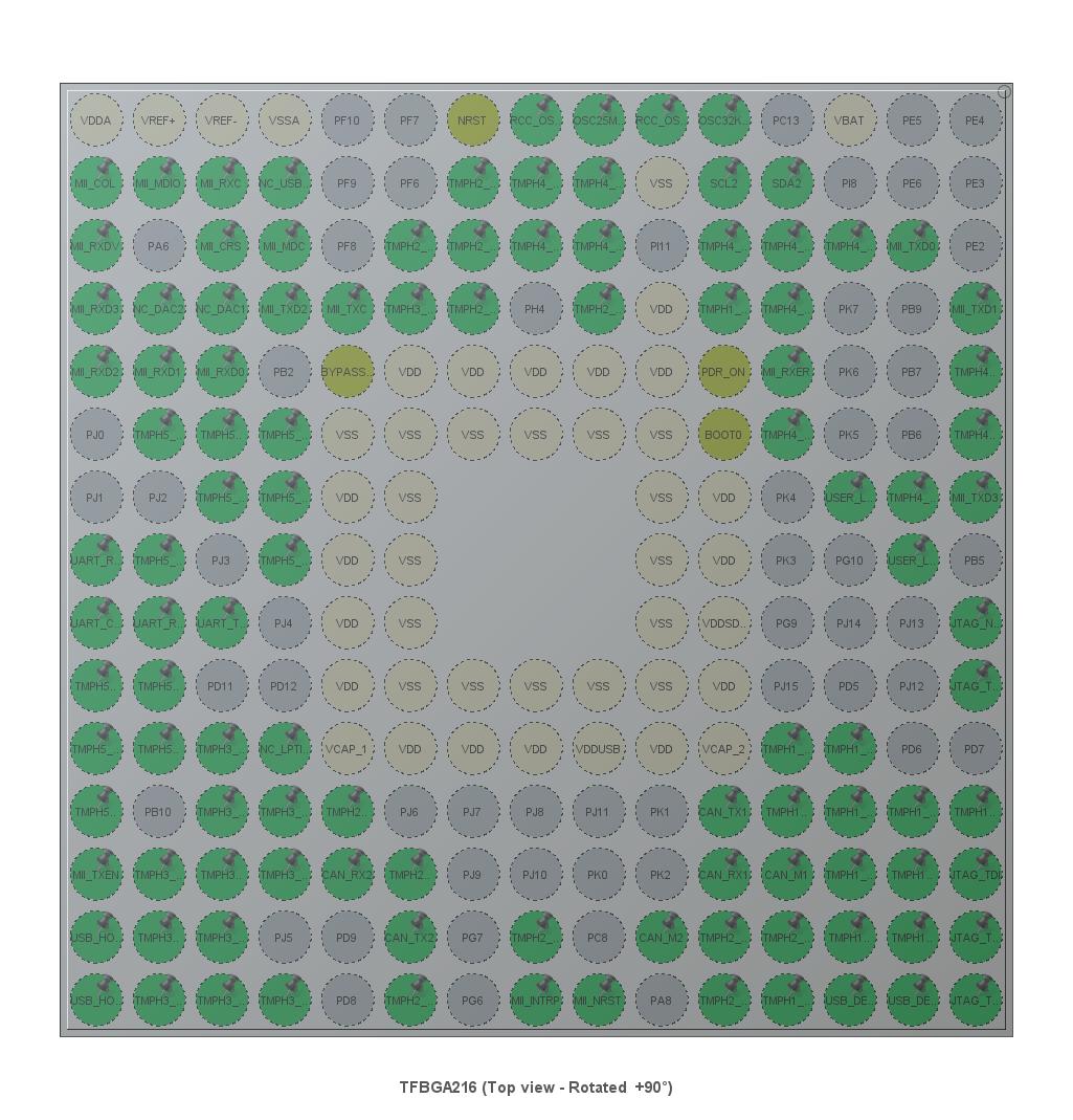
The STM32F7 exposes its various function blocks to the outside of the device through a programmable I/O multiplex matrix on its hundreds of pins. In order to be able to create and modify the configuration data for this matrix in a semantically correct way, the CPU manufacturer provides the tool STM32CubeMX [4]. This tool must then be used with the IOC project file provided by this documentation to edit or export the exact corresponding pin configurations of the given hardware design, e.g. to CSV representation or PDF report:
TiaC Magpie STM32F7 IOC project file:
STM32F777NIHx.iocTiaC Magpie STM32F7 PDF report file:
STM32F777NIHx.pdf
Position |
Name |
Type |
Signal |
Label |
|---|---|---|---|---|
A1 |
PE4 |
I/O |
||
A2 |
PE3 |
I/O |
||
A3 |
PE2 |
I/O |
||
A4 |
PG14 |
I/O |
ETH_TXD1 |
MII_TXD1 |
A5 |
PE1 |
I/O |
UART8_TX |
TMPH4_PE1_TXD8 |
A6 |
PE0 |
I/O |
UART8_RX |
TMPH4_PE0_RXD8 |
A7 |
PB8 |
I/O |
ETH_TXD3 |
MII_TXD3 |
A8 |
PB5 |
I/O |
||
A9 |
PB4 |
I/O |
SYS_JTRST |
JTAG_NTRST |
A10 |
PB3 |
I/O |
SYS_JTDO-SWO |
JTAG_TDO_TRACE_SWO |
A11 |
PD7 |
I/O |
||
A12 |
PC12 |
I/O |
UART5_TX |
TMPH1_PC12_TXD5 |
A13 |
PA15 |
I/O |
SYS_JTDI |
JTAG_TDI |
A14 |
PA14 |
I/O |
SYS_JTCK-SWCLK |
JTAG_TCK_SW_CLK |
A15 |
PA13 |
I/O |
SYS_JTMS-SWDIO |
JTAG_TMS_SW_DIO |
B1 |
PE5 |
I/O |
||
B2 |
PE6 |
I/O |
||
B3 |
PG13 |
I/O |
ETH_TXD0 |
MII_TXD0 |
B4 |
PB9 |
I/O |
||
B5 |
PB7 |
I/O |
||
B6 |
PB6 |
I/O |
||
B7 |
PG15 |
I/O |
GPIO_Analog |
TMPH4_PG15 |
B8 |
PG11 |
Output |
GPIO_Output |
USER_LED1 |
B9 |
PJ13 |
I/O |
||
B10 |
PJ12 |
I/O |
||
B11 |
PD6 |
I/O |
||
B12 |
PD0 |
I/O |
UART4_RX |
TMPH1_PD0_RXD4 |
B13 |
PC11 |
I/O |
USART3_RX |
TMPH1_PC11_RXD3 |
B14 |
PC10 |
I/O |
USART3_TX |
TMPH1_PC10_TXD3 |
B15 |
PA12 |
I/O |
USB_OTG_FS_DP |
USB_DEV_DP |
C1 |
VBAT |
Power |
||
C2 |
PI8 |
I/O |
||
C3 |
PI4 |
I/O |
GPIO_Analog |
TMPH4_PI4 |
C4 |
PK7 |
I/O |
||
C5 |
PK6 |
I/O |
||
C6 |
PK5 |
I/O |
||
C7 |
PG12 |
Output |
GPIO_Output |
USER_LED2 |
C8 |
PG10 |
I/O |
||
C9 |
PJ14 |
I/O |
||
C10 |
PD5 |
I/O |
||
C11 |
PD3 |
I/O |
GPIO_Analog |
TMPH1_PD3 |
C12 |
PD1 |
I/O |
UART4_TX |
TMPH1_PD1_TXD4 |
C13 |
PI3 |
I/O |
GPIO_Analog |
TMPH1_PI3 |
C14 |
PI2 |
I/O |
TIM8_CH4 |
TMPH1_PI2_PWM84 |
C15 |
PA11 |
I/O |
USB_OTG_FS_DM |
USB_DEV_DM |
D1 |
PC13 |
I/O |
||
D2 |
PF0 |
I/O |
I2C2_SDA |
SDA2 |
D3 |
PI5 |
I/O |
TIM8_CH1 |
TMPH4_PI5_PWM81 |
D4 |
PI7 |
I/O |
TIM8_CH3 |
TMPH4_PI7_PWM83 |
D5 |
PI10 |
I/O |
ETH_RX_ER |
MII_RXER |
D6 |
PI6 |
I/O |
TIM8_CH2 |
TMPH4_PI6_PWM82 |
D7 |
PK4 |
I/O |
||
D8 |
PK3 |
I/O |
||
D9 |
PG9 |
I/O |
||
D10 |
PJ15 |
I/O |
||
D11 |
PD4 |
I/O |
GPIO_Analog |
TMPH1_PD4 |
D12 |
PD2 |
I/O |
UART5_RX |
TMPH1_PD2_RXD5 |
D13 |
PH15 |
Output |
GPIO_Output |
CAN_M1 |
D14 |
PI1 |
I/O |
GPIO_Analog |
TMPH2_PI1 |
D15 |
PA10 |
I/O |
GPIO_Analog |
TMPH1_PA10 |
E1 |
PC14/OSC32_IN |
I/O |
RCC_OSC32_IN |
OSC32K_IN |
E2 |
PF1 |
I/O |
I2C2_SCL |
SCL2 |
E3 |
PI12 |
I/O |
GPIO_Analog |
TMPH4_PI12 |
E4 |
PI9 |
I/O |
GPIO_Analog |
TMPH1_PI9 |
E5 |
PDR_ON |
Reset |
||
E6 |
BOOT0 |
Boot |
||
E7 |
VDD |
Power |
||
E8 |
VDD |
Power |
||
E9 |
VDDSDMMC |
Power |
||
E10 |
VDD |
Power |
||
E11 |
VCAP_2 |
Power |
||
E12 |
PH13 |
I/O |
CAN1_TX |
CAN_TX1 |
E13 |
PH14 |
I/O |
CAN1_RX |
CAN_RX1 |
E14 |
PI0 |
I/O |
GPIO_Analog |
TMPH2_PI0 |
E15 |
PA9 |
I/O |
GPIO_Analog |
TMPH2_PA9 |
F1 |
PC15/OSC32_OUT |
I/O |
RCC_OSC32_OUT |
|
F2 |
VSS |
Power |
||
F3 |
PI11 |
I/O |
||
F4 |
VDD |
Power |
||
F5 |
VDD |
Power |
||
F6 |
VSS |
Power |
||
F7 |
VSS |
Power |
||
F8 |
VSS |
Power |
||
F9 |
VSS |
Power |
||
F10 |
VSS |
Power |
||
F11 |
VDD |
Power |
||
F12 |
PK1 |
I/O |
||
F13 |
PK2 |
I/O |
||
F14 |
PC9 |
Output |
GPIO_Output |
CAN_M2 |
F15 |
PA8 |
I/O |
||
G1 |
PH0/OSC_IN |
I/O |
RCC_OSC_IN |
OSC25M_IN |
G2 |
PF2 |
I/O |
GPIO_Analog |
TMPH4_PF2 |
G3 |
PI13 |
I/O |
GPIO_Analog |
TMPH4_PI13 |
G4 |
PI15 |
I/O |
GPIO_Analog |
TMPH2_PI15 |
G5 |
VDD |
Power |
||
G6 |
VSS |
Power |
||
G10 |
VSS |
Power |
||
G11 |
VDDUSB |
Power |
||
G12 |
PJ11 |
I/O |
||
G13 |
PK0 |
I/O |
||
G14 |
PC8 |
I/O |
||
G15 |
PC7 |
Output |
GPIO_Output |
MII_NRST |
H1 |
PH1/OSC_OUT |
I/O |
RCC_OSC_OUT |
|
H2 |
PF3 |
I/O |
GPIO_Analog ADC3_IN9 |
TMPH4_PF3_ADC39 |
H3 |
PI14 |
I/O |
GPIO_Analog |
TMPH4_PI14 |
H4 |
PH4 |
I/O |
||
H5 |
VDD |
Power |
||
H6 |
VSS |
Power |
||
H10 |
VSS |
Power |
||
H11 |
VDD |
Power |
||
H12 |
PJ8 |
I/O |
||
H13 |
PJ10 |
I/O |
||
H14 |
PG8 |
I/O |
GPIO_Analog |
TMPH2_PG8 |
H15 |
PC6 |
I/O |
GPIO_EXTI6 |
MII_INTRP |
J1 |
NRST |
Reset |
||
J2 |
PF4 |
I/O |
GPIO_Analog ADC3_IN14 |
TMPH2_PF4_ADC314 |
J3 |
PH5 |
I/O |
SPI5_NSS |
TMPH2_PH5_NSS5 |
J4 |
PH3 |
I/O |
GPIO_Analog |
TMPH2_PH3 |
J5 |
VDD |
Power |
||
J6 |
VSS |
Power |
||
J10 |
VSS |
Power |
||
J11 |
VDD |
Power |
||
J12 |
PJ7 |
I/O |
||
J13 |
PJ9 |
I/O |
||
J14 |
PG7 |
I/O |
||
J15 |
PG6 |
I/O |
||
K1 |
PF7 |
I/O |
||
K2 |
PF6 |
I/O |
||
K3 |
PF5 |
I/O |
GPIO_Analog ADC3_IN15 |
TMPH2_PF5_ADC315 |
K4 |
PH2 |
I/O |
GPIO_Analog |
TMPH3_PH2 |
K5 |
VDD |
Power |
||
K6 |
VSS |
Power |
||
K7 |
VSS |
Power |
||
K8 |
VSS |
Power |
||
K9 |
VSS |
Power |
||
K10 |
VSS |
Power |
||
K11 |
VDD |
Power |
||
K12 |
PJ6 |
I/O |
||
K13 |
PD15 |
I/O |
UART8_RTS |
TMPH2_PD15_RTS8 |
K14 |
PB13 |
I/O |
CAN2_TX |
CAN_TX2 |
K15 |
PD10 |
I/O |
GPIO_Analog |
TMPH2_PD10 |
L1 |
PF10 |
I/O |
||
L2 |
PF9 |
I/O |
||
L3 |
PF8 |
I/O |
||
L4 |
PC3 |
I/O |
ETH_TX_CLK |
MII_TXC |
L5 |
BYPASS_REG |
Reset |
||
L6 |
VSS |
Power |
||
L7 |
VDD |
Power |
||
L8 |
VDD |
Power |
||
L9 |
VDD |
Power |
||
L10 |
VDD |
Power |
||
L11 |
VCAP_1 |
Power |
||
L12 |
PD14 |
I/O |
UART8_CTS |
TMPH2_PD14_CTS8 |
L13 |
PB12 |
I/O |
CAN2_RX |
CAN_RX2 |
L14 |
PD9 |
I/O |
||
L15 |
PD8 |
I/O |
||
M1 |
VSSA |
Power |
||
M2 |
PC0 |
Output |
GPIO_Output |
NC_USB_HOST_VBUS |
M3 |
PC1 |
I/O |
ETH_MDC |
MII_MDC |
M4 |
PC2 |
I/O |
ETH_TXD2 |
MII_TXD2 |
M5 |
PB2 |
I/O |
||
M6 |
PF12 |
I/O |
GPIO_Analog |
TMPH5_PF12 |
M7 |
PG1 |
I/O |
GPIO_Analog |
TMPH5_PG1 |
M8 |
PF15 |
I/O |
I2C4_SDA |
TMPH5_PF15_SDA4 |
M9 |
PJ4 |
I/O |
||
M10 |
PD12 |
I/O |
||
M11 |
PD13 |
I/O |
LPTIM1_OUT |
NC_LPTIM1 |
M12 |
PG3 |
I/O |
GPIO_Analog |
TMPH3_PG3 |
M13 |
PG2 |
I/O |
GPIO_Analog |
TMPH3_PG2 |
M14 |
PJ5 |
I/O |
||
M15 |
PH12 |
I/O |
GPIO_Analog |
TMPH3_PH12 |
N1 |
VREF- |
Power |
||
N2 |
PA1 |
I/O |
ETH_RX_CLK |
MII_RXC |
N3 |
PA0/WKUP |
I/O |
ETH_CRS |
MII_CRS |
N4 |
PA4 |
I/O |
DAC_OUT1 |
NC_DAC1 |
N5 |
PC4 |
I/O |
ETH_RXD0 |
MII_RXD0 |
N6 |
PF13 |
I/O |
I2C4_SMBA |
TMPH5_PF13_SMBA4 |
N7 |
PG0 |
I/O |
GPIO_Analog |
TMPH5_PG0 |
N8 |
PJ3 |
I/O |
||
N9 |
PE8 |
I/O |
UART7_TX |
UART_TXD7 |
N10 |
PD11 |
I/O |
||
N11 |
PG5 |
I/O |
GPIO_Analog |
TMPH3_PG5 |
N12 |
PG4 |
I/O |
GPIO_Analog |
TMPH3_PG4 |
N13 |
PH7 |
I/O |
I2C3_SCL |
TMPH3_PH7_SCL3_MISO5 |
N14 |
PH9 |
I/O |
GPIO_Analog |
TMPH3_PH9 |
N15 |
PH11 |
I/O |
GPIO_Analog |
TMPH3_PH11 |
P1 |
VREF+ |
Power |
||
P2 |
PA2 |
I/O |
ETH_MDIO |
MII_MDIO |
P3 |
PA6 |
I/O |
||
P4 |
PA5 |
I/O |
DAC_OUT2 |
NC_DAC2 |
P5 |
PC5 |
I/O |
ETH_RXD1 |
MII_RXD1 |
P6 |
PF14 |
I/O |
I2C4_SCL |
TMPH5_PF14_SCL4 |
P7 |
PJ2 |
I/O |
||
P8 |
PF11 |
I/O |
SPI5_MOSI |
TMPH5_PF11_MOSI5 |
P9 |
PE9 |
I/O |
UART7_RTS |
UART_RTS7 |
P10 |
PE11 |
I/O |
SPI4_NSS |
TMPH5_PE11_NSS4 |
P11 |
PE14 |
I/O |
SPI4_MOSI |
TMPH5_PE14_MOSI4 |
P12 |
PB10 |
I/O |
||
P13 |
PH6 |
I/O |
SPI5_SCK |
TMPH3_PH6_SCK5 |
P14 |
PH8 |
I/O |
I2C3_SDA |
TMPH3_PH8_SDA3 |
P15 |
PH10 |
I/O |
GPIO_Analog |
TMPH3_PH10 |
R1 |
VDDA |
Power |
||
R2 |
PA3 |
I/O |
ETH_COL |
MII_COL |
R3 |
PA7 |
I/O |
ETH_RX_DV |
MII_RXDV |
R4 |
PB1 |
I/O |
ETH_RXD3 |
MII_RXD3 |
R5 |
PB0 |
I/O |
ETH_RXD2 |
MII_RXD2 |
R6 |
PJ0 |
I/O |
||
R7 |
PJ1 |
I/O |
||
R8 |
PE7 |
I/O |
UART7_RX |
UART_RXD7 |
R9 |
PE10 |
I/O |
UART7_CTS |
UART_CTS7 |
R10 |
PE12 |
I/O |
SPI4_SCK |
TMPH5_PE12_SCK4 |
R11 |
PE15 |
I/O |
GPIO_Analog |
TMPH5_PE15 |
R12 |
PE13 |
I/O |
SPI4_MISO |
TMPH5_PE13_MISO4 |
R13 |
PB11 |
I/O |
ETH_TX_EN |
MII_TXEN |
R14 |
PB14 |
I/O |
USB_OTG_HS_DM |
USB_HOST_DM |
R15 |
PB15 |
I/O |
USB_OTG_HS_DP |
USB_HOST_DP |