Capacitive Touch Evaluation System for RA2L1
Overview
The RA2L1 MCU Group Capacitive Touch Evaluation System (RTK0EG0022S01001BJ) is a kit created for evaluating the RA2L1 MCU Group Capacitive Touch Sensing Unit (CTSU).
RTK0EG0022S01001BJ is composed of two boards: The RA2L1 Cap Touch CPU Board is mounted with an RA2L1 MCU which includes an on-chip CTSU. The Capacitive Touch Application Board Capacitive Touch Application Board is equipped with self-capacitance touch buttons, wheel and slider electrodes, and LEDs touch electrodes.
Renesas RA2L1 Microcontroller Group has following features
48MHz, Arm Cortex-M23 core
256kB or 128kB Code Flash, 8kB Data Flash, 32kB SRAM (divided on 2 equal areas with- and without- ECC support)
SCI x 5
SPI x 2
I2C x 2
CAN x 1
12-bit A/D Converter
12-bit D/A Converter
Low-Power Analog Comparator x 2
Temperature Sensor
General PWM Timer 32-bit x 4
General PWM Timer 16-bit x 6
Low Power Asynchronous General-Purpose Timer x 2
Watchdog Timer (WDT)
Independent Watchdog Timer (IWDT)
Up to 85 Input/Output pins (depends on the package type)
Hardware
The main functions of the RA2L1 Cap Touch CPU board are as follows:
Renesas RA2L1 MCU Group
R7FA2L1AB2DFP
100-pin LFQFP package
48MHz Arm Cortex®-M23 Core with built-in Arm® MPU (Armv8-M architecture)
32KB SRAM
256KB code flash memory
8KB data flash memory
32-channel capacitive touch sensing unit (CTSU) pins
Connectivity
USB serial conversion interface (FT234XD manufactured by FTDI)
10-pin JTAG/SWD interface for connecting external debugger or programmer (option)
Application board GPIO interface: 2.54mm pitch, 16 pins (8 x 2 DIL)
Application board CTSU interface: 2.54mm pitch, 40 pins (20 x 2 DIL)
Other functions
MCU current measurement jumper
User push button switches: 2
User LEDs: 2
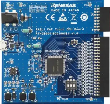
RA2L1 Cap Touch CPU Board (Credit: Renesas Electronics Corporation)
Key functions of the Capacitive Touch Application Board are as follows:
Self-capacitance detection touch electrodes
Buttons: 3
Wheel (4-electrode configuration): 1
Slider (5-electrode configuration): 1
LEDs: 16
Supported Features
The rssk_ra2l1 board supports the hardware features listed below.
- on-chip / on-board
- Feature integrated in the SoC / present on the board.
- 2 / 2
-
Number of instances that are enabled / disabled.
Click on the label to see the first instance of this feature in the board/SoC DTS files. -
vnd,foo -
Compatible string for the Devicetree binding matching the feature.
Click on the link to view the binding documentation.
rssk_ra2l1/r7fa2l1abxxfp target
On-target memory for this board target: 32 KiB of RAM, 256 KiB of Flash.
Type |
Location |
Description |
Compatible |
|---|---|---|---|
CPU |
on-chip |
ARM Cortex-M23 CPU1 |
|
ADC |
on-chip |
Renesas RA 12-bit resolution ADC (ADC12)1 |
|
Clock control |
on-chip |
Renesas RA Clock Generation Circuit external clock configuration1 |
|
on-chip |
Generic fixed-rate clock provider3 |
||
on-chip |
Renesas RA Sub-Clock1 |
||
on-chip |
Renesas RA Clock Control node pclk block1 |
||
on-chip |
|||
Counter |
on-chip |
Renesas RA AGT as Counter2 |
|
CRC |
on-chip |
Renesas RA CRC device1 |
|
DAC |
on-chip |
Renesas RA DAC Controller Global1 |
|
on-chip |
Renesas RA DAC Controller1 |
||
Flash controller |
on-chip |
Renesas RA family flash low-power controller1 |
|
GPIO & Headers |
on-chip |
||
I2C |
on-chip |
Renesas RA SCI I2C controller5 |
|
on-chip |
Renesas RA I2C controller2 |
||
Input |
on-chip |
Renesas RA Capacitive Sensing Unit1 |
|
on-board |
Group of GPIO-bound input keys1 |
||
Interrupt controller |
on-chip |
ARMv8-M NVIC (Nested Vectored Interrupt Controller)1 |
|
LED |
on-board |
Group of GPIO-controlled LEDs1 |
|
Miscellaneous |
on-chip |
Renesas RA Event Link Controller1 |
|
on-chip |
|||
on-chip |
Renesas RA AGT2 |
||
on-chip |
|||
MMU / MPU |
on-chip |
ARMv8-M MPU (Memory Protection Unit)1 |
|
MTD |
on-chip |
Flash memory binding for Renesas RA Code flash region1 |
|
on-chip |
Flash memory binding for Renesas RA Data flash region1 |
||
Pin control |
on-chip |
Renesas RA Pin Controller1 |
|
PWM |
on-chip |
Renesas RA Pulse Width Modulation10 |
|
Reserved memory |
on-chip |
Renesas Option-Setting Memory3 |
|
RNG |
on-chip |
Renesas RA TRNG1 |
|
Serial controller |
on-chip |
||
SPI |
on-chip |
Renesas RA SCI SPI controller5 |
|
on-chip |
Renesas RA SPI controller2 |
||
SRAM |
on-chip |
Generic on-chip SRAM1 |
|
Timer |
on-chip |
ARMv8-M System Tick1 |
|
Watchdog |
on-chip |
Renesas RA Watchdog (wdt)1 |
Programming and debugging
Building & Flashing
You can build and flash an application with an external J-Link debug adapter connect to J1 connector. Building an Application and Run an Application for more details.
Here is an example for building and flashing the Blinky application.
# From the root of the zephyr repository
west build -b rssk_ra2l1 samples/basic/blinky
west flash
Debugging
Debugging also can be done with an external J-Link debug adapter connected to J1 connector. For the debug log output through UART console, you need to connect a USB cable from the host PC to the USB Serial Conversion on CN5. The following command is debugging the Blinky application. Also, see the instructions specific to the debug server that you use.
# From the root of the zephyr repository
west build -b rssk_ra2l1 samples/basic/blinky
west debug
Or you can use Segger Ozone (Segger Ozone Download) for a visual debug interface
Once downloaded and installed, open Segger Ozone and configure the debug project like so:
Target Device: R7FA2L1AB
Target Interface: SWD
Target Interface Speed: 4 MHz
Host Interface: USB
Program File: <path/to/your/build/zephyr.elf>